"Our 14nm delivers a logic transistor density of about 37.5 million transistors per square millimeter. Our 10nm technology delivers about 100 million transistors per square millimeter."
So go draw a square millimeter. For us US people, it's a little bigger than 1/32 of an inch (closer to 1/26th of an inch). If you do any woodworking, you can have a dovetail too big by that much and just wack it in. So it's sort of the allowable slop in a woodworking joint (in softwoods).
They've got 100 million transistors in that tiny amount of space? I know, it's not news, but wow, stop and think about the tech that they have to have to do the layout. Quite an accomplishment, especially considering that the transistor was invented in 1947. In 70 years we go from just having a transistor to having 100 million in a square millimeter.
Other than computer stuff, is there anything else that has seen that sort of scaling up?
My first job out of school was at Sperry Univac in 1985. They had a lab that was a pretty big room (think maybe the size of a grocery store in the US, or maybe half that). I estimated then that the lab probably contained one transistor for every human on the planet.
Now you can get that in 8 mm x 10 mm on a single die. Absolutely amazing.
Also, that first one was quite a bit bigger than 1 mm^2 [1] There's nothing for scale, but standing like that i'd guess 2 or 3 inches across, something like 800 mm^2.
> For the other companies just shipping 10nm, we expect what they call 10nm to have a logic transistor density measured close 50 million transistors per square millimeter, not the 100 million per square millimeter that we offer on our 10nm. It’s almost a full generation difference.
Something to keep in mind. I've read in multiple articles that other foundries have caught up with intel. Apparently not quite. Though it's probably closer than it has been for a while.
> I've read in multiple articles that other foundries have caught up with intel.
This was 100% intentional market warfare by those other companies. Companies needed to make up the ideological gap and Intel took a bit of a stumble, so they decided to fudge the numbers and make it look like they somehow made up a whole generation's progress overnight - think "megahertz wars", only this time worse (basically, the numbers are completely meaningless market monikers now - you're forced to go read the spec sheets.)
I was under the impression the others hadn't quite caught up but were stuck at 14nm and 16nm. Are you saying the nm claims are wrong or is there somthing more complex here in the industry I'm missing? Sorry, I'm not a hardware guy and have lots to learn in the area.
Also not a hardware guy, but the issue seems to revolve around density, intel puts transistors on a chip "like this" the other guys do it "l i k e t h i s". They can make small things, but haven't worked out how to really pack them in next to each other and work reliably.
This isn't really true, there's a lot of marketing misinformation on both sides. Both with Intel and with TSMC/Samsung/GloFo.
The thing is that with "14nm/16nm", the front end of the line (FEOL) was with FinFETs at a "true' 14/16nm density, but the backend of the line (BEOL) and interconnects were at the older node.
But this doesn't necessarily mean that Intel has a moral high ground here, since they've had a lower than industry standard density from "32nm" and "40nm" and below.
TL;DR: "nm" node names are basically useless now, just know that TSMC 10nm isn't a production node and TSMC "7nm" ~= Intel "10nm"
Samsung's 10 nm process is reportedly denser than Intel's 14 nm process, and as Intel and TSMC have not shipped any 10 nm devices yet, this currently gives Samsung a technological lead in terms of density, respectively.[30][31][32]
Intel's "10nm" ~= to TSMC's "7nm", so they are right that their "10nm" is a lot less dense than Intel's "10nm", but they both ship are around the same time, so this means that there's really no difference in terms of time to market.
It's true that the node names are messed up, but Intel acting as if they have the "moore-al high ground" and they "aren't marketers" rubs me the wrong way because from "32nm" and "40nm" and below, Intel's node was far less dense than the industry standard.
> ARM is part of our foundry offerings now. We offer ARM IP, which can be put on Intel chips and be part of an Intel chip, whether it’s a 14nm or 10nm chip. That’s an IP block, not necessarily a separate chip.
Stratix 10 SX SoCs feature hard processor system with 64 bit quad-core ARM Cortex-A53 processor available in all densities in addition to all the features of Stratix 10 GX devices.
Stratix 10 is the latest offering though (very new and expensive), more comparable to what Xilinx refers to as their "UltraScale+ MPSOCs", which are basically their Zynqs, using the UltraScale+ fabric as opposed to Artix/Kintex level stuff, and branded differently.
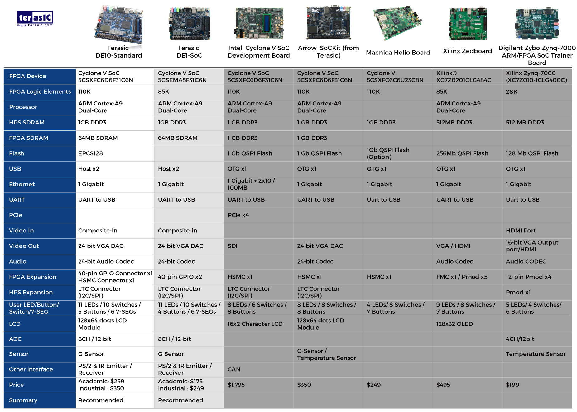
You can get affordable Cyclone V FPGA/ARM boards though, which are more comparable to the traditional "Zynq" series (dual ~1ghz 32bit cores, some DDR3, etc).
I don't know that this is what they're doing, but what I've wanted for several years is a dual power mode computer.
In powered up mode it would operate like a normal x86_64 chip, full power and full speed. But in low power or standby mode it could switch to an ARM chip or core and maintain access to RAM and disks to let it run updates and downloads in the background.
For example, right now to update Windows or Steam games or other software, I have to leave my computer running at full power. Generally depending on what I'm doing I want to throttle or stop the downloads so it doesn't interfere with my normal use. But I also hate leaving my desktop on at full power and with the fans running just so it can do downloads and background tasks.
Or an ARM core could run a simple file server, letting me access files and information stored on my desktop without leaving it on all the time.
TL;DR: I wish I could have an ARM core in my desktop to run background tasks like downloads and other things Raspberry Pi-ish levels of performance.
That's an intriguing concept, but it seems like it would be a headache to implement, from a software perspective. Unless I'm mistaken, if you wanted this low-power chip to perform windows updates, you would need MS to provide an ARM compiled program to perform x86_64 updates. Or you'd need a third party to do it somehow, which sounds messy. The same would apply for anything else you wanted to do that's more complicated than putting files in fixed locations. I suppose it could be relatively easy to just do the downloads, and leave installations/updates for when the main chip kicks in.
And the fileserver concept is pretty neat. Rather than having a separate low power machine that you send files to, your main PC could act as a fileserver using separate software while fully powered or in low-power mode. I'd buy that, if only for the novelty.
It is a fascinating idea. I'm wondering if something like an ARM build of Windows 10 S could already support an ARM to x86_64 handoff with the main kernel/OS/UWP apps running immediately available in low power scenarios and where it might pass things of to Win32 on ARM emulation instead pass things to an x86_64 core? Then from there build out more hand-off capabilities for power hungry processes or performance-hungry apps (like Xbox Game Mode)?
To some extent, I would be surprised if there aren't teams at Microsoft exploring such crazy hybrid notions already, if at least for options for future Xbox or Surface hardware. Recalls to mind Microsoft already experimented with a notification platform of a low power CPU screen coupled to a Windows device way back in the Vista timeframe [1].
The fact that programs are shipped as machine code bytes has plagued computing since the beginning. Security issues and backwards compatibility shackles abound in this model.
The obvious solution to these sort of problems problems is to send programs in some intermediate or high level form, with compilers for local CPUs being part of the loading process. While some successful environments have already done this (notably OS/400, and the ever-up-and-coming Mill CPU), there's just still too much momentum in the popular OSes for the "simpler" binary model.
It would absolutely require some level of Windows/OS support.
While you could definitely allow apps to run arbitrary ARM code on it, I also think it would be quite feasible for the hardware or the OS to expose a simpler API as well with basic functions like 'queue download' that would simply take a protocol, a URL, and a disk location.
ARM has a system they call "big.LITTLE" which essentially works this way: each processor contains pairs of cores, one high-performance core matched up with one low-power core, using a cache-coherent interconnect so that jobs can be swapped back and forth. They're not trying to use heterogeneous ISAs, though, so it's not quite as complicated as what you're describing.
Intel binned that product line a while back; the "ARM GPU" you're thinking of is actually a PowerVR design that Intel licensed to use on the Poulsbo Atom chips.
It was a complete unmitigated disaster. The GPU was slow and had endless driver bugs, and it was made worse by Intel having to negotiate with ImaginationTech for driver support... Not at all surprising Intel stepped up their own GPU game in response.
So go draw a square millimeter. For us US people, it's a little bigger than 1/32 of an inch (closer to 1/26th of an inch). If you do any woodworking, you can have a dovetail too big by that much and just wack it in. So it's sort of the allowable slop in a woodworking joint (in softwoods).
They've got 100 million transistors in that tiny amount of space? I know, it's not news, but wow, stop and think about the tech that they have to have to do the layout. Quite an accomplishment, especially considering that the transistor was invented in 1947. In 70 years we go from just having a transistor to having 100 million in a square millimeter.
Other than computer stuff, is there anything else that has seen that sort of scaling up?